Butterfly wings inspired photovoltaics: Absorption can be increased by up to 200 percent
Nanostructure optimizes light absorption in the butterfly – Principle can be transferred to photovoltaics – Absorption rate as a theoretical upper limit for increasing the efficiency of the solar cell.
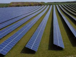
Nanostructures on the wing of Pachliopta aristolochiae can be transferred to solar cells and increase their absorption rates by up to 200% (Graph: Radwanul H. Siddique, KIT / CalTech)
Sunlight reflected from solar cells is lost as unused energy. The wings of the butterfly “Ordinary Rose” (Pachliopta aristolochiae) are characterized by nanostructures, small holes that absorb light more easily than smooth surfaces over a broad spectrum. Researchers at the Karlsruhe Institute of Technology (KIT) have now succeeded in transferring these nanostructures to solar cells and increasing their light absorption rate by up to 200 percent. The scientists have now published their findings in the specialist magazine Science Advances. DOI: 10.1126 / sciadv.1700232
“The butterfly we have examined has an obvious peculiarity: it is extremely dark black. This is due to the fact that it absorbs the sunlight particularly well for optimal heat generation. Even more exciting than its appearance are for us the mechanisms by which it reaches the high absorption. The potential for optimization, which has a transfer of these structures for photovoltaics, was much higher than we had expected, “says Dr. Hendrik Hölscher from the Institute for Microstructure Technology (IMT) at KIT.
The scientists around Hendrik Hölscher and Radwanul H. Siddique (formerly KIT, now CalTech) formed the nanostructures identified at the butterfly on the silicon layer of a thin-film solar cell. The subsequent analysis of the light absorption yielded promising results: compared to a flat surface, the absorption rate increases by 97% with a vertical incidence of incidence and steadily increases until it reaches 207% at an incidence angle of 50 degrees. “This is particularly interesting for European lighting conditions, since diffuse light is often present here and the light is rarely perpendicular to the solar cells,” says Hendrik Hölscher.
Das bedeute allerdings nicht automatisch eine Effizienzsteigerung der gesamten PV-Anlage in gleicher Höhe, so Guillaume Gomard vom IMT. „Auch andere Komponenten spielen eine Rolle. Die 200 Prozent sind daher eher als theoretische Obergrenze für die Effizienzsteigerung zu sehen.“
Vor dem Übertragen der Nanostrukturen auf die Solarzellen ermittelten die Forscher Durchmesser und Anordnung der Nanolöcher auf dem Flügel des Schmetterlings mittels Mikrospektroskopie. Anschließend analysierten sie in einer Computersimulation die Stärke der Licht-Absorption bei unterschiedlichen Lochmustern: Dabei zeigte sich, dass unregelmäßig angeordnete Löcher mit variierenden Durchmessern, so wie sie beim Schmetterling zu finden sind, die stabilsten Absorptionsraten über das gesamte Spektrum und verschiedene Einfallswinkel erzielten. Dementsprechend haben sie die Löcher auf der Solarzelle zufällig und mit unterschiedlichen Durchmessern von 133 bis 343 Nanometern angeordnet.
The scientists have shown with their research that the removal of material can considerably increase the light output. In the project they were working with amorphous silicon, but according to the researchers, any kind of thin film photovoltaic modules could be improved with such nanostructures, even on an industrial scale.
Background information:
Thin-film photovoltaic modules represent an economical alternative to conventional crystalline silicon solar cells, since the light-absorbing layer is up to 1000 times flatter and thus the raw material requirement is considerably smaller. However, the absorption rates of the thin films are lower than those of crystalline cells. This is why they are mainly used where little power is required, such as pocket calculators or wrist- watches. An increase in absorption makes thin-film cells economically attractive even for larger applications such as photovoltaic systems on roofs.
Other materials:
More pictures and graphics
As “The Research University in the Helmholtz Association”, the KIT creates and imparts knowledge for society and the environment. The aim is to make significant contributions to the global challenges in the fields of energy, mobility and information. To this end, around 9,300 employees work together on a broad disciplinary basis in natural sciences, engineering, business, humanities and social sciences. KIT is preparing 26,000 students for research-oriented university studies on responsible tasks in society, business and science. The innovation activity at the KIT is a bridge between knowledge and application for social benefits, economic prosperity and the preservation of our natural resources.


